(Hong Kong)


Product Summary
The Hynix H55S2622JFR-60M is a 256M Mobile SDRAM ideally suited for the main memory applications which requires large memory density and high bandwidth. It is organized as 4banks of 2,097,152 x32. The H55S2622JFR-60M is designed for non-PC application which use the batteries such as PDAs, 2.5G and 3G cellular phones with internet access and multimedia capabilities, mini-notebook, hand-held PCs.
Parametrics
Absolute maximum ratings: (1)Ambient Temperature, TA: -30 ~ 85 ℃; (2)Storage Temperature, TSTG: -55 ~ 125 ℃; (3)Voltage on Any Pin relative to VSS, VIN, VOUT: -1.0 ~ 2.6 V; (4)Voltage on VDD relative to VSS, VDD: -1.0 ~ 2.6 V; (5)Voltage on VDDQ relative to VSS, VDDQ: -1.0 ~ 2.6 V; (6)Short Circuit Output Current, IOS: 50 mA; (7)Power Dissipation, PD: 1 W; (8)Soldering Temperature . Time, TSOLDER: 260 . 20℃.
Features
Features: (1)Standard SDRAM Protocol; (2)Clock Synchronization Operation: All the commands registered on positive edge of basic input clock (CLK); (3)MULTIBANK OPERATION - Internal 4bank operation: During burst Read or Write operation, burst Read or Write for a different bank is performed; During burst Read or Write operation, a different bank is activated and burst Read or Write for that bank is performed; During auto precharge burst Read or Write, burst Read or Write for a different bank is performed; (4)Power Supply Voltage: VDD = 1.8V, VDDQ = 1.8V; (5)LVCMOS compatible I/O Interface; (6)Low Voltage interface to reduce I/O power; (7)Programmable burst length: 1, 2, 4, 8 or full page; (8)Programmable Burst Type: sequential or interleaved; (9)Programmable CAS latency of 3 or 2; (10)Programmable Drive Strength; (11)Low Power Features.
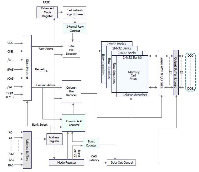
Diagrams